|
A Nuclear Microbattery for MEMS Devices |
A. LAL, R. M. BILBAO Y LEÓN, H. GUO, H. LI, S. SANTANAM, R. YAO, J. BLANCHARD, D. HENDERSON. |
University of Wisconsin - Madison |
|
1500 Engineering Drive, Madison, WI 53706 |
|
blanchard@engr.wisc.edu |
Keywords: Power, Radiation
Abstract
Microelectromechanical Systems (MEMS) have not gained wide use because they lack the on-device power required by many important applications. Several forms of energy could be considered to supply this needed power (solar, fossil fuels, etc), but nuclear sources provide an intriguing option in terms of power density and lifetime. This paper describes several approaches for establishing the viability of nuclear sources for powering realistic MEMS devices. Isotopes currently being used include alpha and low-energy beta emitters. The sources are in both solid and liquid form, and a technique for plating a solid source from a liquid source has been investigated. Several approaches are being explored for the production of MEMS power sources. The first concept is a junction-type battery. The second concept involves a more direct use of the charged particles produced by the decay: the creation of a resonator by inducing movement due to attraction or repulsion resulting from the collection of charged particles. Performance results are provided for each of these concepts.
Microelectromechanical Systems (MEMS) comprise a rapidly expanding research field with potential applications varying from sensors in airbags to more recent optical applications. Depending on the application, these devices often require an on-board power source for remote operation, especially in cases requiring operation for an extended period of time. Previously suggested power sources include fossil fuels and solar energy, but nuclear power sources may provide significant advantages for certain applications. Hence, the objective of this study is to establish the viability of nuclear sources (beta and alpha particles) for powering realistic MEMS devices. This approach has previously been used to make large-scale batteries and has the advantage that very high voltages at low power are easily generated.
For example, a common method of actuation of surface micromachines is the use of electrostatic forces between microscopic parallel plates. Such actuation techniques require voltages on the order of 50 to 100 V for useful plate movements of tens of microns. Although these voltages are high, power in the range of only nanowatts to microwatts is needed to run surface micromachines. Voltage sources that produce voltages in this range are too large and negate the advantage of making electromechanical systems at the microscale. For realizing truly autonomous microscale electromechanical systems one needs to make integrated microbatteries on the same substrate as the micromachines. Although several groups have tried to fabricate microbatteries using on-chip liquid-state or solid-state electrochemical cells, they typically only produce a few volts. Integration of transforming circuits to realize high voltages requires inefficient energy conversion and chip area loss. Hence, integration of direct-charging nuclear batteries that produce high voltages with surface micromachined MEMS devices has great potential for advancing the value of MEMS devices. Such integration will enable microscale systems to be used for a number of very important applications.
This work explores the viability of several base designs for such power sources, thus demonstrating the feasibility of producing nuclear, on-board power sources for MEMS devices.
A critical aspect of the creation of microbatteries for MEMS devices is the choice of the isotope to be used as a power source. Some requirements for this isotope include safety, reliability, cost, and activity. Since the size of the device is an issue in this particular application, gamma emitters have not been considered because they would require a substantial amount of shielding. Both pure alpha and low energy beta emitters have been used. The alpha emitters have an advantage due to the short range of the alpha particles. This short range allows increased efficiency and thus provides more design flexibility, assuming that a sufficient activity can be achieved. The half-life of the isotopes must be high enough so that the useful life of the battery is sufficient for typical applications, and low enough to provide sufficient activity. In addition, the new isotope resulting after decay should be stable, or it should decay without emitting gamma radiation. The isotopes currently in use for this work are:
|
Isotope |
Radiation Type |
Half-Life |
Max Energy [keV] |
Average Energy [keV] |
|
3H |
Beta |
12.3 y |
18.6 |
5.7 |
|
63Ni |
Beta |
100.2 y |
66.9 |
17.4 |
|
210Po |
Alpha |
138.4 d |
5304.3 |
- |
Table 1: Isotopes used for this work.
To explore the viability of the nuclear microbattery concept, some scoping calculations need to be carried out. Using 210Po as an example, one can analyze the best case scenario, assuming that the nuclear battery is created using pure 210Po. In this case, the activity would be approximately 4,500 Ci per gram or 43,000 Ci per cubic centimeter. Thus, for a characteristic source volume of 10-5 cubic centimeters (0.1 cm x 0.1cm x 10 microns), one obtains approximately 0.5 Ci. Based on the results of previous experimental studies, the available power would be on the order of 0.5 mW (about 1 mW/Ci). The power required for MEMS devices can range from nanowatts to microwatts. A typical case is that of a low power CMOS driven mechanical cantilever forming an air-gap capacitor with the substrate. Typical MEMS capacitors have 10 femtoFarad capacitance and resonant frequencies of 10s of kHz. The power dissipated for charging such an electromechanical capacitor would be in the range of 10 to 100 nanowatts. Therefore, a pure source provides more than sufficient activity to power a practical device.
Three methods of incorporating radioactive material into the MEMS devices are being studied. These are 1) activation of layers within the MEMS device, 2) addition of liquid radioactive material into fabricated devices, and 3) addition of solid radioactive material into fabricated devices.
In the first approach, the parent material for the radioactive daughter or granddaughter would be manufactured as part of the MEMS device, most likely near the surface of the device. After fabrication of the device, the parent material would be exposed to the radiation field in our TRIGA reactor for a period of time until the desired radiation source strength is achieved. Highly absorbing neutron or charged particle materials would be used to mask other components of the device which are to remain non-radioactive. In addition, the material used for the activation would be chosen such that it has a high activation cross-section, thus maximizing the activation of the “source” and minimizing competing activity produced in surrounding structures.
In the second and third approaches, radioactive sources are introduced into the MEMS device after fabrication. In the case of a liquid source, a reservoir must be created within the device, along with a channel providing access to the reservoir. The reservoir can then be filled, relying on capillary action to create the flow, and the channel can then be sealed off if needed.
In the case of a solid source, the radioactive material will have to be deposited in selected sites on the device. We currently have two approaches to create this type of sources:
§ Electroless Plating of 63Ni:
Electroless plating is the plating of nickel without the use of electrodes but by chemical reduction [1]. Metallic nickel is produced by the chemical reduction of nickel solutions with hypophosphite using an autocatalytic bath. The plating metal can be deposited in the pure form on to the plated surfaces. The bath is an aqueous solution of nickel salt and contains relatively low concentration of hypophosphite. This type of nickel plating can be used on a large group of metals, such as steel, iron, platinum, silver, nickel, gold, copper, cobalt, palladium and aluminum.
Throughout the plating process, the bath needs to be heated to maintain it at a temperature in the range of 90 – 100 °C to promote the chemical reduction reaction. The boiling temperature of the bath is to be avoided. At lower temperatures the reaction proceeds slowly and at higher temperatures the bath evaporates. The important factor influencing the plating process is the pH. The pH needs to be maintained at 4.5-6 for plating to occur. A lower pH results in no plating at all.
We have successfully plated gold-coated silicon pieces of dimensions 2mm by 2mm, following this procedure. Plating of nickel on gold was observed in about 15 minutes. These solid sources can then be incorporated into a MEMS device.
§ 3H Microspheres
We have obtained glass microspheres (25 to 53 µm in diameter) that will emit low energy 3H beta radiation. These are obtained by irradiating 6Li glass silicate non-radioactive microspheres in the UW Nuclear Reactor. Using this procedure, we can produce activities of up to 12.8 mCi per gram and per hour of irradiation. Then, these radioactive microspheres can be introduced in the MEMS device in the appropriate cavity.
These latter approaches will allow for higher power densities than the direct reactor activation approach, but will provide less flexibility with respect to device design. We are currently exploring the tradeoffs of the different options, and will shortly release all the data needed to assess the viability of all of these approaches.
Since this work involves the use of small amounts of radiation and radioactive materials, it is necessary to comply with current Radiation Protection Standards [2][3]. The potential health and environmental effects of fabricating, using and disposing of these nuclear micro-batteries have been studied in detail.
Current radiation protection regulations are based on the Linear Non-Threshold model (LNT), which assumes that any amount of radiation exposure, no matter how small, may have negative health effects. This model was derived by extrapolating known acute (high dose and high dose rate) exposure data points in a linear or curvilinear fashion through the origin. Lately, however, there has been a movement among the Medical and Health Physics communities encouraging the review of the current regulations by using the Non-Linear Threshold model (NLT), that establishes that there are no detectable harmful health effects to humans at radiation levels below 100 mSv (10 rem). Therefore, even though we will prove that our devices do comply with current regulations, the actual health effects may be even more insignificant.
§ Manufacturing Process
Our analysis demonstrates that the potential amounts of radiation that a worker could be exposed to due to the fabrication of these nuclear microbatteries are well below the limits established by current laws. Our study includes the external exposure as well as the internal exposure due to ingestion or inhalation of the radioactive materials.
The manufacturing process will be designed keeping the radiological safety of the workers in mind, but the costs incurred upon due to the extra security measures needed to handle radioactive materials and radioactivity will be reasonable so that the final price of the micro-batteries is competitive.
§ Use
MEMS devices, with their integrated nuclear micro-battery will be used in large variety of applications, as sensors, actuators, resonators, etc. It will be ensured that their use does not result in any unsafe exposure to radiation. The radioactive material in the device will be encapsulated in a way that the probability of being released into the environment, and being accidentally inhaled or digested is extremely small. However, the analysis has been performed in the worst case scenario, assuming that the full amount of the radioactive material contained by the microbattery would be accidentally ingested or inhaled.
For obvious reasons, in addition to safety considerations, the design of the shielding and encapsulation of these microdevices is aimed to minimize the size and weight of the devices, and their cost.
The external dose associated with these sources is zero, because an alpha particle needs to have an energy of more than 7.5 MeV to penetrate the protective layer of the skin (0.07 mm think), and a ß particle needs to have an energy of more than 70 keV. Since our sources have energies lower than those they are unable to penetrate the skin.
|
|
INHALATION |
INGESTION |
||
|
DOSE LIMIT [2] [mrem/d] |
44.57 |
5.479 |
||
|
3H |
2.4 |
18 |
0.0346 |
158 |
|
64Ni |
5.69 |
7 |
0.0813 |
67 |
|
210Po |
13540 |
- |
193.4 |
- |
|
DOSE EQUIV. TO LUNG [mrem/d] |
# OF DEVICES INHALED TO REACH THE LIMIT |
DOSE EQUIV. TO WHOLE BODY [mrem/d] |
# OF DEVICES INGESTED TO REACH THE LIMIT |
|
Table 2: Radiation Effects on a worker after the inhalation or ingestion of a 5 μCi micro-battery.
|
|
INHALATION |
INGESTION |
||
|
DOSE LIMIT [2] [mrem/d] |
2.28 |
0.273 |
||
|
3H |
2.4 |
0.95 |
0.0346 |
7 |
|
64Ni |
5.69 |
0.40 |
0.0813 |
3 |
|
210Po |
13540 |
- |
193.4 |
- |
|
|
DOSE EQUIV. TO LUNG [mrem/d] |
# OF DEVICES INHALED TO REACH THE LIMIT |
DOSE EQUIV. TO WHOLE BODY [mrem/d] |
# OF DEVICES INGESTED TO REACH THE LIMIT |
Table 3: Radiation Effects on a member of the public after the inhalation or ingestion of a 5 μCi micro-battery.
§ Waste Disposal
Our analysis proves that the environmental impact of disposing of these micro-devices once their useful life has ended, as well as the associated costs are minimal. Since after three half-lives the activity of the isotope has decayed to about 10% of the original activity, the micro-batteries would be below background radiation level at the following times:
|
Isotope |
Half-Life |
Time to 10% if Initial Activity |
|
3H |
12.3 y |
36.9 y |
|
63Ni |
100.2 y |
300.6 y |
|
210Po |
138.4 d |
1.1 y |
Table 4: Time needed by different radioisotopes to decay under 10% of their original activity.
The electron-voltaic effects were studied extensively in the 1950’s and it was found that beta particles with energies below 250 keV do not cause substantial damage in silicon [4][5]. Therefore, liquid 63Ni was selected as the radioactive source for these tests, since its maximum and average energies (66.9 keV and 17.4 keV respectively) are well below the threshold energy where damage is observed in silicon. In addition, its long half-life (100 year) makes it very attractive for remote long-life applications, such as power of spacecraft instrumentation.
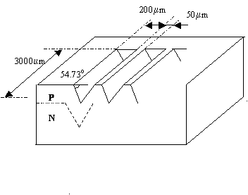
Figure 1: Diagram of a micromachined pn-junction
Since it is not easy to microfabricate solid radioactive materials (etching and cutting), a liquid source is used instead for our micromachined pn-junction battery. As shown in Figure 1, a number of bulk-etched channels have been micromachined in our pn-junction. Compared with conventional planar pn-junctions, the three dimensional structure of our device allows for a substantial increase of the junction area, and the micromachined channels can be used to store the liquid source. Our pn-junction has 13 micromachined channels and the total junction area is 15.894 mm2 (about 55.82% more than the planar pn-junction). This can be very important since the current generated by the powered pn-junction, whether it is powered by light or by a nuclear source, is proportional to the junction area. Figure 2 shows the I-V curve of our pn-junction due only to the interaction of light, as measured by a semiconductor parameter analyzer.
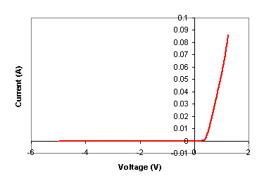
Figure 3. I-V curve of a micromachined pn-junction powered by the light.
In order to measure the performance of our three-dimensional pn-junction in the presence of a radioactive source, we use a pipette to place 8 µl of liquid 63Ni source (64 µCi) inside the channels micromachined on top of the pn-junction, and then we cover it with a black box to shield it from the light. The electric circuit used for these experiments is shown in Figure 3.
We obtain the I-V curve by varying the resistance R and using the ammeter to measure the current for each resistance value. It is worth noting that the voltage across the pn-junction is equal to the voltage across the adjustable resistance, which is equal to the product of the resistance R and the current flowing through.
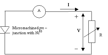
Figure 3: Electric circuit for experiments with micromachined pn-junction and 63Ni.
Figure 4 displays the I-V curves measured at 30 minutes, 2 hours and 16 hours after pouring the radioactive source on the microchannels of the pn-junction. As expected, the degradation of the pn-junction due to the 63Ni is very small. However, to conclusively demonstrate this extreme would require a longer testing time, comparable to the expected life of the nuclear micro-battery.
In Figure 4, we observe that the maximum current generated in the micromachined pn-junction by the 63Ni source, i.e. the short circuit current, is 1.31 nA. In silicon, the generation of one Electron-Hole Pair (EHP) requires about 3.2 eV, even though its energy gap between the conduction band and covalence band is just 1.12 eV. So the theoretical maximum current generated by 64µCi can be calculated as:
Imax = 64 µCi * (3.7*1010 dps) * (17.4 keV) / (3.2 eV) * (1.6*10-19 C) = 2.06*10-9 A = 2.06 nA
According to this estimate, the measured current value is 64.07% of the theoretical maximum value. This illustrates the effectiveness of making the boron diffused depth around 40µm during microfabrication, which is approximately the traveling distance of 63Ni beta particles in silicon. Normal pn-junctions, which have ultra shallow junctions (less than 1µm), would result in very low currents since most of the beta particles would stop in the p or in the n regions, instead of the depletion region.
On the other hand, the open circuit voltage is very small, only 53 mV. This is partly due to the large p and n contact resistances. In this particular device, the metal used for the p contact is gold and for the n contact is aluminum alloy, and both the p and n regions are all covered by metal (the open circuit voltage for a normal junction-type battery is in the range of 0.2 to 0.5 V). A very effective way of increasing the open circuit voltage in a junction-type battery is by reducing the contact area.
The maximum power can be approximately estimated by:
Pmax = Is * Vo= 1.31 nA * 0.053 V = 0.069 nW
Further research on improving the device design and its performance is still on the way and will be released in the near future.
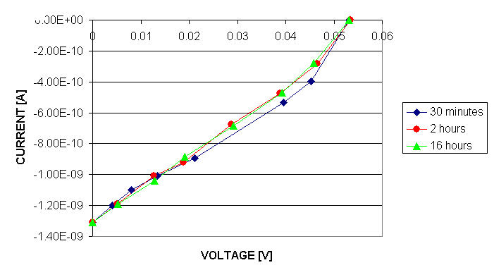
Figure 4: I-V curves for a micromachined pn-junction with 63Ni at different times
This concept involves a more direct use of the charged particles produced by the decay of the radioactive source: the creation of a resonator by inducing movement due to attraction or repulsion resulting from the collection of charged particles. As the charge is collected, the deflection of a cantilever beam increases until it contacts a grounded element, thus discharging the beam and causing it to return to its original position. This process will repeat as long as the source is active.
This concept has been tested experimentally with positive results. Figure 5 shows the experimental setup, in which the charges emitted from the source are collected in the beam to generate the electrostatic force that drives it. The radioactive source used was 63Ni with an activity of 1 mCi. The beam is 5 cm ´ 5 mm, made from 60 mm thick copper. A probe tip is glued to the beam to better detect and measure the movement of the beam. Both the source and the beam are mounted on a glass base for electrical insulation. The glass base is clamped so that the beam itself can only move by bending. The measuring scale is a silicon beam with 3mm spaced gridlines so that the movement can be measured with a precision of 1.5mm. A CCD camera connected to a VCR is used to record the movement of the beam and its periodicity.
As the radioactive beta source decays, it emits electrons. The copper beam collects these electrons from the source, and the source itself would become positively charged since it keeps losing electrons; therefore, in the ideal case, there would be an electrostatic force applied on the beam that would bend it. However, in atmospheric conditions, no movement of the beam is observed, due to the ionization of the surrounding air. For that reason, the experiment has been performed under vacuum (typically from 30 mTorr to 50 mTorr), where there is no extraneous ionization and the bending of the beam can be observed.
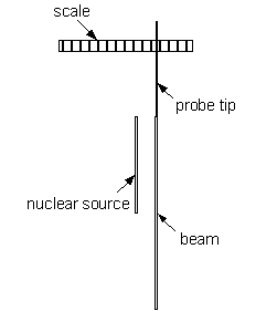
Figure 5: Self-Reciprocating Cantilever Experimental Set-up
In order to understand the behavior of the system we have developed an analytical model for both the charge collection and deflection of the cantilever. The charge collecting process is governed by:
![]()
where dQ is the amount of charge collected by the beam during a given time dt, a represents the current emitted by the radioactive source, V is the voltage across the source and the beam and R is the effective resistance between them. The second term on the right hand side represents the current leakage arising from the ionization of the air. Since V = Q / C, where C is the capacitance of the beam and the source, the previous equation can be rearranged to obtain:
![]()
Figure 6 shows a typical experimental result, in which the initial distance is 3.5 mm and the vacuum is 50 mTorr.
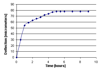
Figure 6: Deflection vs. time at a pressure of 50 mTorr
This equation can be readily solved:
![]()
In Figure 6 we observe that the beam bends very slowly. Therefore, the electrostatic force on the beam can be taken as balanced by the elastic force from the beam itself. Since the electrostatic force is proportional to Q2 and the distance between the beam and the source can be taken as a constant, being d the deflection of the beam, we have:
![]()
K is the elastic constant of the beam, a can be assumed to be constant since 63Ni has a half life of more than 100 years, R in the experiment is also a constant because the pressure is maintained and no breakdown of the air happened, otherwise the beam will bounce back. C can also be assumed to be constant because it has been observed experimentally that the deflection of the beam is very small compared to the initial distance between the beam and the radioactive source. Therefore
![]()
Figure 7 compares the deflection measured experimentally with the values obtained analytically according to the discussion shown above, by fitting R. We observe a very good match between them.
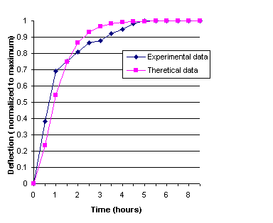
Figure 7: Comparison between the experimental and analytical values for the deflection.
This model, however, does not include the periodic behavior of this device. Current experiments show a minimum period of about 30 minutes, at which time the electrostatic energy is released as electric current. Further studies are being done in this area, trying to identify the key characteristics of the system in order to be able to design the device with the period and energy release level appropriate for each particular application.
A junction-type battery was constructed using Si and a 63Ni liquid source. A source volume containing 64 µCi was poured into 13 micromachined channels to increase the surface area contacted by the source. The measured current was approximately 1.3 nA (about 64% of the theoretical maximum) at 0.05 V, giving a power of about 0.07 nW.
A more novel application of nuclear sources for MEMS applications involves the creation of a resonator, which is driven by charge collection in a cantilever beam. Preliminary results have established the feasibility of this concept and future work will optimize the design for various applications.
A recipe for electroless plating of Nickel has been successfully applied to the plating of non-radioactive Nickel on gold. We will soon use the same recipe to plate 63Ni in a MEMS device.
This work is supported by the US DOE under NEER grant DE-FG07-99ID13781
"Symposium on Electroless Nickel Plating", ASTM Special Technical Publication No. 265, American Society for Testing Materials, Philadelphia, PA, 1959.
"Recommendations of the International Commission on Radiological Protection Report", ICRP publication 60. Elmsford, N.Y., Pergamon Press, 1990.
" Standards For Protection Against Radiation". Title 10, Code of Federal Regulations, Part 20, Nuclear Regulatory Commission, Washington, D.C. Continuosly updated. (http://www.nrc.gov/NRC/CFR/PART020/).
J.J.Loferski and P.Rappaport, “Electron Voltaic Study of Electron Bombardment Damage and Its Threshold in Ge and Si,” Phys. Rev., Vol.98, p.1861,June,1955
P.Rappaport, and J.J.Loferski, “Thresholds for Electron Bombardment Induced Lattice Displacements in Si and Ge,” Phys. Rev., Vol.100,p.1261,November,1955